APT system enables three-dimensional characterization of materials at atomic resolution, providing precise identification of the position and composition of individual atoms with exceptionally high chemical sensitivity.
It is suitable for a wide range of materials – including metals, ceramics, semiconductors, and biomaterials – and serves as a complementary tool to advanced electron microscopy.
There is a paramount importance today in Israel for the APT to meet the requirements of resolution and spatial identification of individual atoms in characterization of advanced materials for energy. The APT Center at the National Institute for Energy Storage will contribute to a better and more comprehensive understanding of the atomic structure, properties, and unique characteristics of materials intended for development in the energy field. Advanced microscopy techniques based on electron and ion beams can address many of these needs, but they are generally limited to two-dimensional information and cannot provide complete data from nanoscale regions while maintaining high chemical sensitivity.
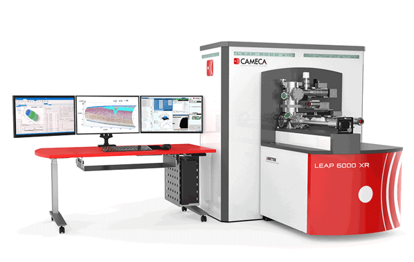
APT is based on field ionization and essentially involves atom-by-atom field evaporation from the surface of a sharp, needle-like specimen with a radius of curvature <40 nanometers. The evaporated ions are accelerated due to high voltage in a ultra-high vacuum chamber toward a multi-channel plate (MCP) detector sensitive to their position (X, Y) and flight time (t), thus relating to the original positions of ions (x, y, z) in the sample. This enables three-dimensional reconstruction of the analyzed volume. The chemical identity of the identified ions is determined by their mass-to-charge state ratio, evaluated from their flight time, accelerating voltage, and flight distance. Beyond the capabilities described, the device can accurately identify different isotopes with precise resolutions.
APT main features include:
- Atomic Resolution: Resolves individual atoms and their positions.
- 3D Imaging: Creates 3D models of nanoscale structures.
- High Sensitivity: Detects elements down to parts-per-million (ppm) concentrations; High detection efficiency for low-atomic mass elements
- Versatility: Applicable for metals, semiconductors, ceramics, and even biomaterials.
The following list outlines major research areas and technologies where APT will play a major role:
- Advanced alloy design for magnesium- and silicon-based rechargeable batteries, utilizing nanoscale coatings.
- Elemental distribution analysis in semiconductors such as silicon and germanium for PV cells, as well as in nanowires used in lithium-ion batteries.
- Characterization of interfaces with complex topologies and advanced chemical and physical properties in fuel cell materials.
- Study of flexible solar cells incorporating organic dye materials.
- Mapping of defect distributions in materials for energy conversion.
- Analysis of nanomaterials used in energy storage applications.
The list of applications and uses for this revolutionary imaging device is extensive and spans additional examples of its impact on materials research and regulations for electrochemical energy storage or energy derived from “green hydrogen” technology. Substantial impacts of such a flagship technology are expected on all energy-related research and its peripheral areas to be conducted in the future in the State of Israel.
Assoc. Prof. Yaron Amouyal
Academic Supervisor
073-3781915
[email protected]
Dr. Inbar Freilich
Manager the center for Atom Probe Tomography (APT)
073-3785135
[email protected]